-
[IT | 기술] (블룸버그) 미중 반도체 경쟁, 첨단 반도체 패키징으로 확대2023.11.21 PM 04:38
블룸버그 기사 요약 (ChatGPT)
미국과 중국 간의 기술 전쟁은 반도체 산업에서 점차 중요해지고 있는 첨단 칩 패키징 분야로 확대되었습니다. 미국은 반도체 생산을 강화하고 아시아 공급망에 대한 의존도를 줄이기 위해 노력을 기울이고 있는 반면, 중국은 첨단 패키징을 활용하여 자국의 반도체 생산 능력을 확대하고 있습니다. 과거에는 종종 간과되었던 이 분야는 이제 더 높은 성능을 달성하고 다양한 유형의 칩을 원활하게 통합하는 데 필수적이라고 간주됩니다.
두 국가 모두 첨단 패키징의 잠재력을 인정합니다. 이 분야는 제재 대상이 아니며 컴퓨팅 성능을 향상시키는 데 필수적입니다. 차세대 반도체 기술에서 뒤처지고 있음에도 불구하고 중국은 첨단 패키징을 이러한 차이를 해소하고 다양한 칩 기술을 효율적으로 결합하는 수단으로 보고 있습니다. 반대로 미국은 이 분야에서 역량을 강화하기 위해 노력하고 있으며 칩 제조를 국내로 되돌리려는 노력을 방해할 수 있다는 점을 인정합니다.
첨단 패키징에 대한 관심은 특히 인공 지능과 같은 애플리케이션을 위한 고성능 반도체를 구동하는 데 필수적이라는 점에서 비롯됩니다. 이는 인공지능 반도체 생산에 병목 현상을 유발하고 있으며, TSMC 및 Intel과 같은 주요 업체들이 전 세계적으로 첨단 패키징 시설 구축에 수십억 달러를 투자하도록 유도하고 있습니다.
산업계는 Moore's Law라고 불리는 칩 발전의 전통적인 경로에 한계에 직면하고 있는 상황에서 첨단 패키징이 해결책으로 부상하고 있으며, 이는 단일 칩에 모든 기능을 집적하는 대신, 여러 칩을 모듈식으로 연결하여 성능을 향상시키는 방식입니다.
첨단 패키징의 중요성은 반도체 산업의 지형을 재구성하는 데 중요한 역할을 하기 때문에 업계 전문가와 정책 입안자들은 점차 그 중요성을 인정하고 있습니다. 미국과 중국은 모두 첨단 칩 패키징이 미래 반도체 제조에 중심적인 역할을 하는 것을 인정하고 이 분야에서 우위를 차지하기 위해 경쟁하고 있습니다.
====================================================
(Bloomberg) A New Front Is Opening Up in the US-China Conflict Over Chips
The emerging field of advanced packaging is being hailed as an inflection point for the semiconductor industry. China is moving in on the same arena.

By Jane Lanhee Lee, Ian King, Mackenzie Hawkins, and Jillian Deutsch
2023년 11월 21일 오전 10:01 GMT+9
President Joe Biden has adopted a two-pronged approach to constrain China’s high-tech progress, curbing Beijing’s access to leading-edge chips while bolstering semiconductor production in the US.
He’s about to ratchet up the pressure further, shifting focus to an emerging arena of the contest for technological supremacy: the process of packaging semiconductors that’s increasingly seen as a path to achieving higher performance.
Not only the US recognizes the potential of so-called advanced packaging; China, too, is capitalizing on this area, which isn't subject to sanctions. It's capturing global market share and making progress in manufacturing high-end chips, a realm previously denied to it.
“Packaging is the new pillar of innovation in the semiconductor industry – it will change the industry drastically,” said Jim McGregor, founder of technology analysts Tirias Research. For China, which doesn’t yet have state-of-the-art capabilities, “it’s definitely easier for them to ramp up” here, since it isn’t restricted by the US government. “Packaging could help them bridge the gap,” he said.
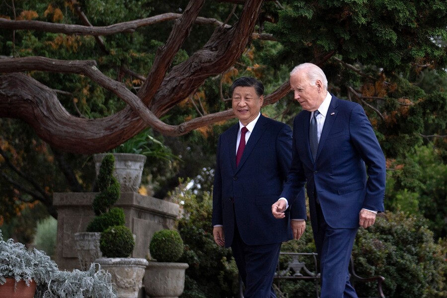
Xi Jinping with Joe Biden in California on Nov. 15.
Photographer: Brendan Smialowski/AFP/Getty Images
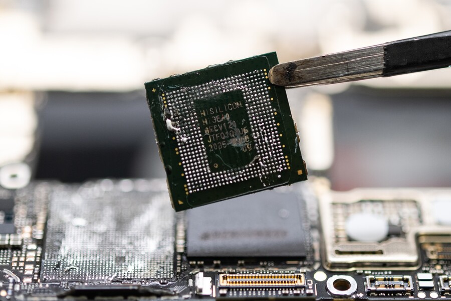
Up until very recently, the business of packaging semiconductors – encasing chips in materials that both protect them and connect them to the electronic device they’re part of – was, at best, an afterthought for the industry. So it was outsourced, mainly to Asia, with China a prime beneficiary: today, the US accounts for just 3% of the world’s packaging capacity, according to Intel Corp.
Yet suddenly, advanced packaging is everywhere: Intel is banking on it as a core part of the US chip giant’s strategy to return to competitiveness; China sees it as a means of building out domestic semiconductor capacity; and now Washington is turning to it as part of its own plans for self-sufficiency.
More than a year after the CHIPS and Science Act came into being, the Biden administration has outlined plans for a $3 billion National Advanced Packaging Manufacturing Program, after recently tapping a director for the center.The goal is to create multiple high-volume packaging facilities by the end of the decade, said Under Secretary of State of Commerce Laurie Locascio — and reduce reliance on Asian supply lines that pose a security risk the US “just can’t accept.”
The president “has made it a priority to ensure America’s leadership in all elements of semiconductor manufacturing, of which advanced packaging is one of the most exciting and critical areas,” a White House official said.
With advanced packaging rapidly becoming a new front in the global conflict over chips, some argue it’s long overdue.
The administration has until now focused on subsidies to bring back chipmaking to the US, but “we can’t ignore packaging because you can’t do one without the other,” said Representative Jay Obernolte, a California Republican who is one of two vice-chairs of the Congressional Artificial Intelligence Caucus. “It wouldn’t matter if we did 100% of our chip manufacturing onshore if the packaging is still offshore,” he added.
Assembly, testing and packaging – usually considered together as “back-end” manufacturing - was always the least glamorous end of the semiconductor industry, with less innovation and lower added value than the “front end” business of making chips with features measured in the billionths of a meter. Yet the level of sophistication is rising fast as new technologies enable chips to be combined, stacked and their performance enhanced in what industry executives are calling an inflection point.
Advanced packaging can’t help China compete with leading-edge semiconductor developments from the U.S., but it allows Beijing to build faster, cheaper systems for computing by stitching together different chips closely together. In that case China could save its latest chip technology, which is expensive and likely available in limited volume, for the most important part of the chip and use older, cheaper technologies to make chips that carry out other functions like battery management and sensor controls, combining the whole in a powerful package.
It's a “pivotal solution,” said Bloomberg Intelligence technology analyst Charles Shum. “It doesn’t merely enhance chip-processing speed but crucially enables seamless integration of varied chip types.” As a result, he said, it’s “set to reshape the semiconductor-manufacturing landscape.”
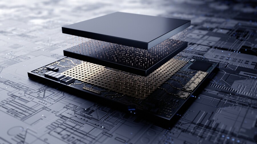
An illustration of Samsung’s 3D packaging technology, known as eXtended-Cube (X-Cube), showing how chiplets are stacked vertically. Source Samsung
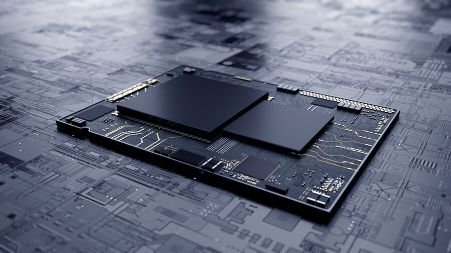
Samsung's X-Cube technology showing chiplets aligned horizontally in a single package. Source: Samsung
Beijing has long made a strategic priority of semiconductor packaging technologies, including in President Xi Jinping’s Made in China program announced in 2015. China has 38% of the world’s assembly, testing and packaging market, the most of any nation, according to the US-based Semiconductor Industry Association. While it lags behind Taiwan and the US in advanced technology, analysts agree that unlike in wafer processing, it’s in a much better p-osition to be able to catch up.
China already boasts the most back-end facilities by number, including the world’s third-largest assembly and testing company, JCET Group, which trails only Taiwan’s ASE Group and Amkor Technology of the US in revenue. What’s more, Chinese companies are building market share, including through JCET’s acquisition of an advanced facility in Singapore and construction of an advanced packaging plant in its hometown of Jiangyin.
“For China, one way around technology transfer restrictions is advanced packaging, because so far it’s a safe space that everyone invests in,” said Mathieu Duchatel of the Institut Montaigne think tank, a Taiwan-based China expert who studies the geopolitics of technology.
It’s a realization now touching Washington as it seeks to deny Beijing access to the kind of advanced computing technologies that could be put to military use – with questionable success.
When Huawei Technologies Inc. quietly released its Mate 60 Pro smartphone in September, China hawks in Washington raised questions as to why US export controls had failed to prevent a development supposedly beyond Beijing’s capabilities.
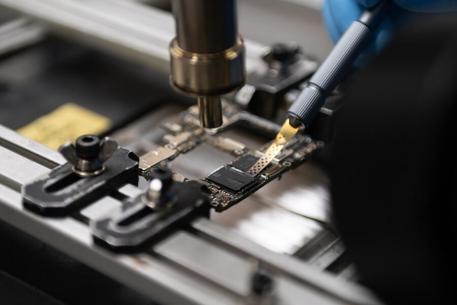
A specialist removes the SMIC chip from a Huawei Mate 60 Pro smartphone in Ottawa, Canada, on Sept. 3.
Photographer: James Park/Bloomberg
In testimony to the House Sept. 19, Commerce Secretary Gina Raimondo defended the Biden administration’s focus on denying China access to leading-edge chips and the equipment to make them. But she was primed on advanced packaging. The US needs to ramp up its own advanced packaging capacities, she said, since “chips can only get so small, which means all the special sauce is in the packaging.”
One reason for the sudden focus on that special sauce is its necessity to the kind of high-power semiconductors needed for artificial intelligence applications. Indeed, a shortage of a particular type of packaging known as Chip on Wafer on Substrate, or CoWoS, is a key bottleneck in the production of Nvidia Corp’s AI chips.
Taiwan Semiconductor Manufacturing Co., the main chipmaker for Nvidia, this summer committed $3 billion to a packaging plant to help alleviate the blockage. CEO C.C. Wei told investors on the company’s third-quarter earnings call that the company planned to double CoWoS capacity by the end of next year.
While TSMC has been working on the technology for 12 years, it was a niche application that only took off this year, Jun He, Vice President of Advanced Packaging Technology, told a conference in Taipei in October. “We’re building capacity like crazy,” said Jun He, adding that “everybody, probably even in Starbucks,” is talking about CoWoS.
It’s not just TSMC. Micron Inc. is setting up a $2.75 billion back-end facility in India, while Intel agreed to build a $4.6 billion assembly and test plant in Poland and is putting some $7 billion into advanced packaging in Malaysia. South Korea’s SK Hynix said last year that it plans to invest $15 billion in a packaging facility in the US.

TSMC’s new factory in Kikuyo, Japan, on May 8.
Photographer: Toru Hanai/Bloomberg
Intel has “some very unique technology now in the packaging area,” Chief Executive Officer Pat Gelsinger said in an interview. “Everybody who’s doing AI chip work today is looking to say, wow, this is the way that I can advance my AI chip capabilities.”
That has some analysts predicting a bonanza for companies in the sphere. According to McKinsey, high-performance chips for data centers, AI accelerators, and consumer electronics will create the greatest demand for advanced packaging technologies.
The number of chips shipped that use advanced packaging is forecast to increase tenfold in the next 18 months – but that could soar to 100 times if it becomes standard in smartphones, Jeffries analysts Mark Lipacis and Vedvati Shrotre wrote in a Sept. 14 report that classed the technology as part of a “tectonic shift” in the industry.
The reason, alluded to by Raimondo, is that chipmaking is running up against the limits of physics.
Chips have been getting better over the last fifty years in large part through advances in production technology. The components now contain up to tens of billions of the tiny transistors that give them the ability to store or process information. But now that path of advancement, called Moore’s Law after Intel’s founder, is coming up against fundamental barriers that are making improvements more difficult and vastly expensive to achieve.
Moore’s Law – more of an observation – states that the number of transistors on a chip doubles about every two years. As that pace of progress slows, and companies “are not able to deliver twice the transistors, at half the cost, at twice the clock speed, and at lower power levels every two years, the industry has begun to rely more on advanced packaging techniques to pick up the slack,” Lipacis and Shrotre wrote.
Instead of cramming ever more tiny components on to one piece of silicon, many designers and companies are touting the benefits of a modular approach, of building products out of several “chiplets” tightly packed together in the same package.

A presentation at the BE Semiconductor Industries booth at the Semicon Taiwan exhibition in Taipei, in September 2022.
That explains why Dutch specialist BE Semiconductor Industries NV, which makes the tools used for chip packages, has doubled its value to some $9.8 billion in the past 12 months, outpacing the Philadelphia Semiconductor Index two-fold despite a slump in the chip industry in the second half of this year.
That’s still dwarfed by the kind of sums involved in front-end manufacturing – fellow Dutch firm ASML NV, which has a near monopoly on the machines needed to produce leading-edge semiconductors, has a market cap approaching $250 billion. Intel’s cutting-edge chip fabrication plant in the eastern German city of Magdeburg has a price tag of $30 billion, or more than four times its Malaysia commitment.
Yet between Magdeburg, a new site in Ireland, and its Polish plant with capacity for advanced packaging, “Poland could actually be the most important,” Gelsinger said.
Chinese companies are piling into the space, too. They include Semiconductor Manufacturing International Corp. – China’s largest chipmaker, which made the 7 nanometer chip powering the Mate 60 Pro – along with IP leader VeriSilicon and Huawei, according to Berlin-based researchers Jan-Peter Kleinhans and John Lee.
These companies “see potential in utilizing advanced packaging processes to achieve performance gains without relying on foreign cutting-edge front-end processes,” Kleinhans and Lee, of the Stiftung Neue Verantwortung think tank and East West Futures consultancy respectively, wrote in a December report.
A Kirin 9000s chip fabricated in China by SMIC, taken from a Huawei Mate 60 Pro smartphone.
Photographer: James Park/Bloomberg
The US Commerce Department justifies its decision to focus on front-end manufacturing on the grounds that sanctioning assembly, test and packaging (APT) services would disrupt supply chains without reducing national security risks. China’s APT services “now play a critical and indispensable role in the global supply chain,” and “cannot easily be substituted,” Commerce’s National Institute of Standards and Technology said in September.
The irony is that luring the likes of TSMC and Samsung Electronics Co. to construct cutting-edge chip plants in Arizona and Texas doesn’t ensure self-reliance, since the current lack of capacity means the advanced wafers those plants produce will need to be shipped to Asia to be packaged – most likely in Taiwan.
For Jack Hergenrother, vice president of IBM Global Enterprise Systems Development, advanced packaging is relatively “overlooked” in funding terms. He wants double the allocation to help spur a rise in US packaging capacity to 10-15% of the global total, and ideally to take 25% in a decade, to ensure a secure supply chain. “Having a hub in North America for advanced packaging is super important,” he said.
— With assistance from Debby Wu and Jordan Fabian